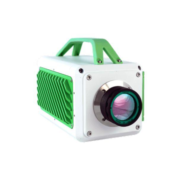
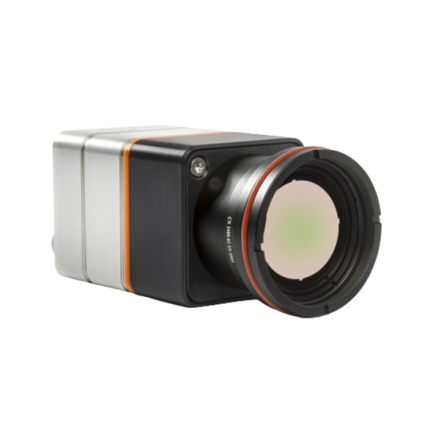
In the semiconductor and solar industries, quality inspection is crucial to ensuring the reliability and performance of end products. Advanced infrared imaging technologies, such as SWIR and photon emission microscopy, play a vital role in detecting defects and impurities in materials like silicon and semiconductor wafers. By identifying flaws early in the manufacturing process, these inspection techniques help optimize product yield and reduce potential failures, ultimately supporting efficient, high-quality production. Our advanced imaging solutions, utilizing UV, SWIR, and LWIR technologies, deliver early defect detection to ensure superior wafer quality. By addressing imperfections early, we help optimize production efficiency, reduce rework costs, increase yield, and maximize throughput, ultimately enhancing equipment ROI.
From UV to LWIR, our comprehensive wavelength capabilities provide the versatility needed for precise semiconductor inspection.
- UV (Ultraviolet 190 to 400 nm): Delivers unmatched precision for detecting microscopic surface defects at the nanometer scale.
- SWIR (Short-Wave Infrared 0.9 to 1.7μm): Leverages silicon’s transparency for precise alignment in stacking, bonding, and packaging.
- LWIR (Long-Wave Infrared 8 to 12μm): Monitors thermal patterns and ensures uniformity, enabling real-time process adjustments and reducing downtime.
Need some answers? Ask our experts!
Contact usInfrared Semiconductor Inspection
Infrared semiconductor inspection optimizes manufacturing processes by identifying and localizing defects, ensuring high-quality production at wafer, die, and packaged device levels.
Photon Emission Microscopy: This advanced failure analysis technique, utilizing SWIR InGaAs detectors, detects photonic radiation from defects caused by carrier recombination, enabling precise and efficient flaw localization.
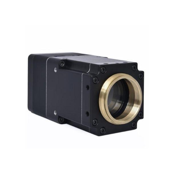
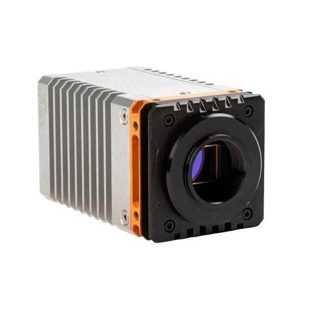
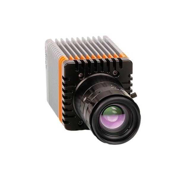
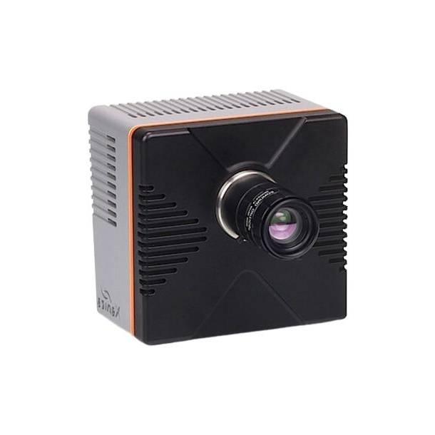
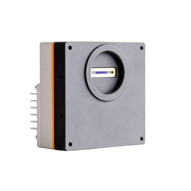
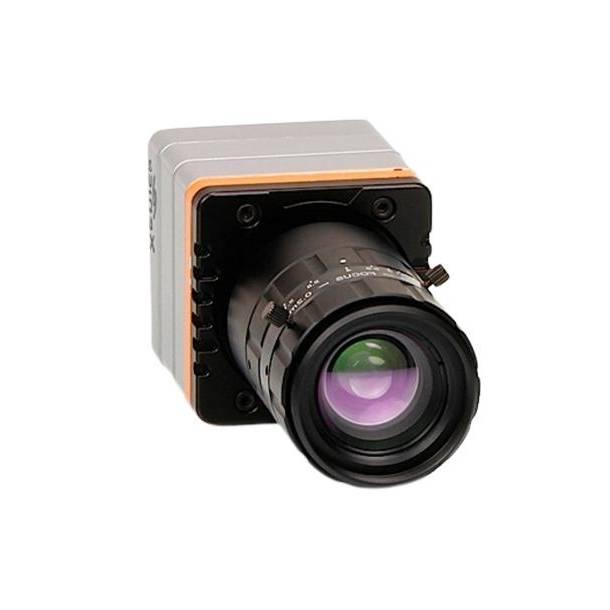
Solar Ingot Inspection: Impurities, voids, and inclusions in silicon bricks and ingots can lead to component failures. SWIR InGaAs cameras (Cheetah+, Wildcat+, Bobcat+, Manx, Lynx) easily detect such defects using light sources emitting wavelengths over 1150 nm, as silicon's transparency to longer SWIR photons allows inspectors to see through ingots.
Thermal Inspection: LWIR cameras (Ceres T series) detect thermal defects and ensure uniform temperature distribution during wafer production, enhancing quality control.
Our SWIR and LWIR cameras provide efficient, reliable tools for defect detection and process optimization, ensuring smoother and higher-quality semiconductor production.
UV cameras for wafer inspection
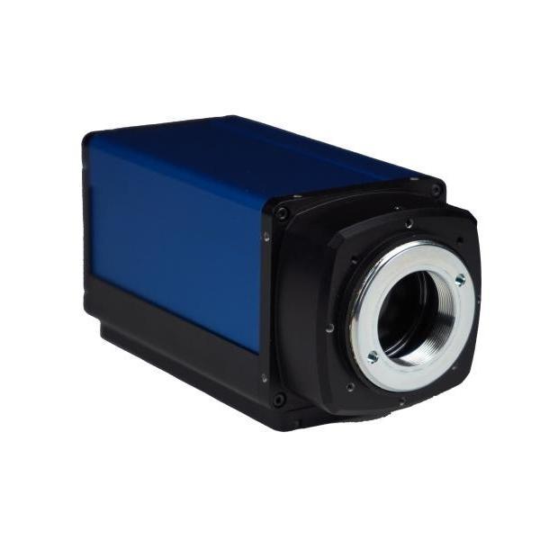
UV cameras are an excellent tool for wafer inspections, offering advanced capabilities for semiconductor applications. Our UV cameras (iNocturn, i2Nocturn) operate in the 190–400 nm range, capturing light beyond the visible spectrum to reveal the undetectable phenomena. These intensified cameras excel at detecting microscopic defects and residues across various colors, depending on the light source, ensuring components meet stringent industry standards.
Unique applications of UV cameras for wafer inspections:
- Darkfield wafer surface inspection
- Defects detection in mask and inline wafer inspection
- Layer thickness inspecting using spectral ellipsometry technique
